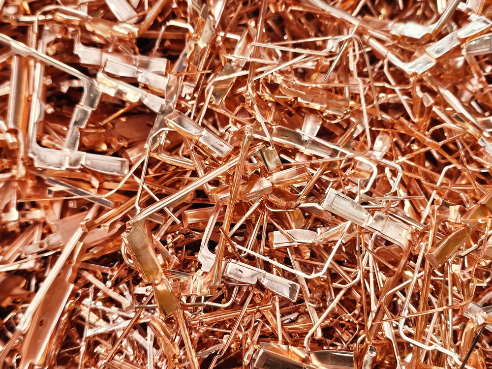
Copper is one of the most valuable metals in modern manufacturing. Its excellent electrical conductivity, thermal performance, corrosion resistance, and formability make it essential for producing components used in electrical systems, electronics, automotive assemblies, telecommunications, and industrial equipment.
However, turning copper into a reliable finished component requires more than choosing the right material. Manufacturers must account for material thickness, alloy composition, tooling design, dimensional tolerances, and production volume. These decisions directly affect part performance, manufacturing costs, and long-term reliability.
Copper metal stamping provides an efficient way to transform copper sheets and coils into precision components. Using specialized dies and mechanical presses, manufacturers can cut, bend, form, and shape copper into parts with consistent dimensions and repeatable quality.
From simple electrical contacts to complex copper terminals and connectors, metal stamping supports both high-volume manufacturing and specialized industrial applications.
Understanding the materials, processes, benefits, and applications of copper stamping can help engineers, purchasing managers, and product designers make informed manufacturing decisions.
What Is Copper Metal Stamping?
Copper metal stamping is a manufacturing process that uses stamping presses and precision tooling to transform flat copper material into finished or partially finished components.
The process typically begins with copper sheet, strip, or coil stock. A stamping press applies controlled force through a die to cut, punch, bend, or form the material into a specific shape.
Depending on the part design, a manufacturer may perform several operations during one press cycle or use multiple stages to achieve the required geometry.
Common copper stamped components include electrical terminals, connectors, busbar components, grounding contacts, conductive clips, brackets, and electronic hardware.
Unlike machining, which removes material using cutting tools, stamping primarily uses shearing and plastic deformation to create the desired shape. This distinction makes stamping particularly attractive when manufacturers need large quantities of identical components.
How Copper Stamping Differs From Other Metal Forming Methods
Copper components can be produced through machining, casting, forging, and several other manufacturing methods. Each process has advantages, but stamping is especially effective for parts made from relatively thin, flat stock.
For example, a copper electrical terminal may require a precisely located mounting hole, a formed contact area, and a narrow profile. A stamping die can perform these operations efficiently, often within a progressive production sequence.
Machining may be more appropriate when a component requires substantial thickness, deep internal features, or complex three-dimensional geometry that cannot be formed economically from sheet material.
Copper stamping is generally preferred when part geometry, production volume, and material requirements support repeatable press operations.
Why Copper Is an Excellent Material for Metal Stamping
Copper offers a combination of physical and mechanical properties that few other metals can match.
Its performance advantages extend beyond electrical conductivity. Copper is also relatively ductile, transfers heat efficiently, and can be manufactured in different tempers to meet specific forming requirements.
Excellent Electrical Conductivity
One of copper’s most important characteristics is its ability to conduct electricity efficiently.
Copper has an electrical conductivity of approximately 100% IACS (International Annealed Copper Standard) when measured against the reference conductivity of annealed copper. Actual conductivity varies by alloy, temper, and material condition.
This property makes copper an excellent choice for components that carry electrical current.
Stamped copper parts are commonly used in:
- Electrical connectors and terminals
- Power distribution systems
- Grounding components
- Switches and contact assemblies
- Battery connections
- Electrical control equipment
High electrical conductivity helps reduce resistive losses, although component performance also depends on contact resistance, geometry, surface condition, and operating temperature.
High Thermal Conductivity
Copper transfers heat efficiently, making it useful for components exposed to elevated temperatures or designed to dissipate thermal energy.
Stamped copper components may be incorporated into heat spreaders, thermal contacts, power electronics, and other equipment where effective heat transfer is important.
In electrical assemblies, copper’s thermal conductivity can also help distribute heat generated by current flow.
Excellent Formability and Ductility
Copper can undergo significant plastic deformation without fracturing when the appropriate alloy, temper, tooling, and forming conditions are used.
This characteristic allows manufacturers to create bends, flanges, tabs, and other formed features.
Annealed copper is particularly well suited for demanding forming operations because it offers greater ductility than harder tempers.
However, copper work-hardens during deformation. Manufacturers must consider this behavior when designing parts with tight bends or multiple forming operations.
Natural Corrosion Resistance
Copper develops a protective surface film when exposed to the atmosphere. This contributes to its corrosion resistance in many environments.
For electrical components, however, corrosion resistance and electrical contact performance are not necessarily the same.
Oxidation and surface contamination can increase contact resistance, particularly in low-force electrical connections.
Manufacturers may specify tin, nickel, silver, or other surface finishes when contact reliability, solderability, or environmental protection is critical.
Long-Term Durability
Properly designed copper components can provide dependable service over extended periods.
Durability depends on several factors, including the selected copper alloy, operating temperature, mechanical loading, exposure conditions, and whether the part experiences repeated bending or vibration.
For components that require spring action or sustained contact force, a copper alloy may perform better than commercially pure copper.
Types of Copper Materials Used in Metal Stamping
Not all copper materials behave the same way during stamping.
Manufacturers select copper grades and alloys based on electrical conductivity, mechanical strength, corrosion resistance, forming requirements, and cost.
The material’s temper is equally important because it influences hardness, ductility, and springback.
C110 Copper: Electrolytic Tough Pitch Copper
C110 copper, commonly called Electrolytic Tough Pitch (ETP) copper, is one of the most widely used grades for electrical applications.
It typically contains at least 99.90% copper and offers excellent electrical and thermal conductivity.
C110 is frequently selected for stamped electrical components because it combines strong conductive performance with good formability.
Typical applications include electrical terminals, busbar components, grounding straps, conductive plates, and power distribution hardware.
The material is available in different tempers, allowing manufacturers to balance forming characteristics with strength requirements.
C101 Copper: Oxygen-Free Electronic Copper
C101 is a high-purity, oxygen-free copper grade commonly used in applications with demanding conductivity and material purity requirements.
It typically contains at least 99.99% copper.
C101 provides excellent electrical and thermal conductivity and is useful in specialized electronic, electrical, and vacuum-related applications.
Its higher material cost means it is generally selected when its specific characteristics provide a measurable advantage over more conventional copper grades.
C102 Copper: Oxygen-Free Copper
C102 copper is another oxygen-free grade with excellent conductivity and formability.
It is used in electrical components and applications where oxygen content must be carefully controlled.
C102 can also be appropriate for certain high-temperature joining or processing conditions where oxygen-bearing copper may present limitations.
For most general electrical stamping applications, the decision between C101, C102, and C110 should be based on actual performance requirements rather than material purity alone.
Copper Alloys Used in Precision Stamping
Pure copper is not always the best choice.
Some stamped components require greater mechanical strength, wear resistance, or spring performance than commercially pure copper can provide.
Copper alloys offer alternative property combinations.
| Material | Key characteristics | Common applications |
|---|---|---|
| C110 copper | Excellent conductivity and good formability | Electrical terminals, grounding parts, busbar components |
| C101 copper | High purity and excellent conductivity | Specialized electrical and electronic components |
| C102 copper | Oxygen-free composition and excellent conductivity | Electrical contacts and specialized assemblies |
| Brass | Good formability, moderate conductivity, and useful strength | Connector hardware, terminals, fittings |
| Phosphor bronze | Good spring properties, fatigue resistance, and wear performance | Spring contacts, clips, connectors |
| Beryllium copper | High strength and excellent spring performance after suitable processing | Precision contacts and spring components |
The correct material depends on the component’s function.
For example, a power distribution component may prioritize electrical conductivity, while a spring contact must maintain consistent mechanical pressure over repeated operating cycles.
How Copper Temper Affects Stamping Performance
Copper temper describes the material’s mechanical condition, often established through cold working or annealing.
Softer tempers generally offer greater ductility, making them useful for complex forming operations.
Harder tempers provide increased strength but typically have less forming capability and may produce greater springback.
A part requiring several tight bends may benefit from softer copper stock. A relatively flat electrical component that needs dimensional stability may use a harder temper.
Engineers should evaluate the required material condition early in the design process because changing temper can affect tooling, tolerances, and part performance.
How the Copper Metal Stamping Process Works
Copper stamping involves several coordinated manufacturing steps. While the exact production sequence varies by component, most projects follow a similar progression from material selection through final inspection.
1. Part Design and Engineering Review
The process begins with a detailed part drawing or CAD model.
Engineers evaluate the component’s dimensions, tolerances, material thickness, bend requirements, hole locations, and intended application.
They also assess whether the part can be manufactured efficiently using stamping equipment.
Design considerations may include minimum bend radii, edge distances, material grain direction, tooling clearance, and the relationship between formed features.
Identifying potential manufacturing problems during the design stage helps prevent costly tooling revisions later.
2. Copper Material Selection
Once the part requirements are established, the manufacturer selects the appropriate copper grade, temper, and stock thickness.
Material selection influences nearly every subsequent operation.
For example, softer copper may simplify bending but increase handling and distortion concerns. Harder material may improve strength while requiring additional attention to springback and tooling stresses.
Copper is commonly supplied as sheet or coil stock, depending on the stamping process and production requirements.
3. Tool and Die Design
Stamping dies determine the shape, dimensional accuracy, and repeatability of finished components.
Tooling may include punches, cutting sections, forming stations, pilots, guides, and other features designed for the part.
Die designers must account for copper’s ductility, material flow, and tendency to produce burrs or adhere to tooling under certain conditions.
Proper punch-to-die clearance is particularly important.
Excessive clearance can create large burrs and poor edge quality, while insufficient clearance can increase cutting forces and accelerate tool wear.
4. Stamping and Forming
During production, copper stock is positioned inside the stamping press.
The press drives the tooling through a controlled stroke, applying sufficient force to shear or deform the material.
Depending on the operation, the tooling may create holes, remove material, form bends, or produce the complete component.
For progressive die stamping, the copper strip advances through multiple stations. Each station performs a specific operation until the finished part is separated from the strip.
5. Secondary Manufacturing Operations
Some copper components require additional processing after stamping.
These operations may include machining, welding, deburring, surface finishing, or assembly.
For instance, a stamped copper component may need a machined feature that cannot be produced economically in the die.
Other parts may require welded connections or finishing operations to remove sharp edges and improve handling.
Coordinating secondary operations with the stamping process helps manufacturers maintain dimensional consistency and reduce unnecessary handling.
6. Inspection and Quality Control
Finished copper components must meet the requirements established in the engineering drawing.
Quality control may include dimensional inspection, visual examination, material verification, and application-specific testing.
Critical electrical components may also require conductivity or contact-resistance testing when specified.
For high-volume production, manufacturers may use statistical process control and scheduled inspections to identify process variation before it affects large quantities of parts.
Common Copper Metal Stamping Techniques
Different stamping methods are used depending on component geometry, material thickness, tooling requirements, and production volume.
Progressive Die Stamping
Progressive die stamping is especially effective for high-volume production of copper components.
A continuous strip of copper moves through a series of stations within one die. Each station performs a different operation, such as piercing, blanking, bending, or forming.
The component remains attached to the carrier strip until the appropriate stage of production.
Progressive stamping offers several advantages, including high production rates, consistent part geometry, and reduced manual handling.
It is frequently used to manufacture electrical terminals, connector contacts, clips, and other small precision components.
Compound Die Stamping
Compound dies perform multiple cutting operations during a single press stroke.
For example, a compound die may create the outside profile of a copper part while simultaneously punching internal holes.
This approach can provide accurate relationships between cut features and is often suitable for relatively flat components.
Transfer Die Stamping
Transfer stamping moves individual workpieces between forming stations.
Unlike progressive stamping, the part does not necessarily remain connected to a continuous strip throughout the process.
Transfer tooling may be appropriate for components requiring more complex forming operations or configurations that are difficult to produce using a carrier strip.
Blanking and Piercing
Blanking and piercing are fundamental sheet metal cutting operations.
Blanking removes a defined shape from the surrounding material. The removed piece typically becomes the desired component.
Piercing creates holes or openings in the workpiece.
Both operations are commonly used to manufacture copper electrical contacts, mounting plates, terminals, and other precision parts.
Bending and Forming
Bending changes the angle or profile of copper stock without intentionally removing material.
Forming operations can create flanges, channels, tabs, offsets, and other features.
Because copper work-hardens, the amount of deformation must be considered carefully.
For demanding geometries, manufacturers may adjust the material temper, bend radius, forming sequence, or tooling design to prevent cracking and dimensional problems.
Deep Drawing
Deep drawing uses a punch to pull sheet material into a die cavity, producing a hollow or cup-shaped component.
Copper’s ductility makes certain grades and tempers suitable for drawing operations.
However, successful deep drawing depends on material properties, blank geometry, lubrication, tooling design, and the required draw depth.
Complex components may require multiple drawing stages or intermediate annealing.
Benefits of Copper Metal Stamping for Industrial Manufacturing
Copper stamping offers advantages that extend beyond material performance.
When the component is designed appropriately, stamping can provide a highly efficient production method with predictable quality and competitive unit costs.
Consistent Dimensional Accuracy
Precision tooling enables manufacturers to produce large quantities of parts with repeatable dimensions.
Once a stamping process is properly established, the same die can produce consistent features across many production cycles.
Actual achievable tolerances depend on part geometry, stock thickness, material condition, tooling, and process capability.
Cost-Effective High-Volume Production
One of the strongest advantages of copper stamping is its production efficiency.
Although custom tooling requires an initial investment, that cost can be distributed across the total production quantity.
As volume increases, the tooling cost per component generally decreases.
Stamping can also reduce labor requirements by performing multiple operations within a single automated process.
For recurring production programs, these efficiencies can make stamping more economical than manufacturing each component individually.
Efficient Material Utilization
Copper is a valuable raw material, so minimizing waste can significantly affect manufacturing costs.
Careful strip layout and part nesting help reduce the amount of unused material.
Progressive die design can also improve material utilization by arranging parts efficiently within the available strip width.
Some scrap is unavoidable, particularly around pierced holes and irregular profiles. However, copper scrap is generally recyclable, allowing manufacturers to recover some material value.
Fast Production Cycles
Automated stamping equipment can produce components at high rates once tooling and process parameters are established.
Production speed depends on part complexity, press capabilities, material feeding requirements, and quality considerations.
For simple components, stamping can support substantially higher production volumes than processes requiring extensive individual machining.
Design Flexibility
Copper stamping can produce a wide variety of component shapes.
Manufacturers can combine cutting, forming, and secondary operations to create parts that meet specific mechanical and electrical requirements.
This flexibility supports everything from simple conductive plates to complex connector components with multiple bends and contact features.
Compatibility With Secondary Operations
Stamped copper components can be integrated into larger manufacturing workflows.
Depending on the application, parts may undergo machining, welding, tumbling, deburring, plating, or assembly.
This compatibility allows manufacturers to produce components that meet both dimensional and functional requirements.
Industrial Applications of Copper Metal Stamping
Copper stamped parts are used throughout industries that depend on reliable electrical connections, efficient heat transfer, and precise metal components.
Electrical and Power Distribution Equipment
Electrical manufacturing is one of the largest application areas for stamped copper components.
Copper’s high conductivity makes it suitable for transferring current between electrical devices and assemblies.
Common components include busbar connections, electrical terminals, conductive plates, grounding contacts, and switch components.
In power distribution applications, engineers must consider current-carrying capacity, temperature rise, joint resistance, and mechanical fastening requirements.
Stamped copper parts can provide consistent geometry while supporting reliable electrical connections.
Electronics and Telecommunications
Electronic devices frequently use small, precision-stamped copper and copper alloy components.
These parts may include connector contacts, shielding components, terminal elements, and conductive hardware.
Dimensional consistency is particularly important because small variations can affect assembly fit and electrical contact performance.
For connectors requiring repeated mating cycles, manufacturers often select copper alloys that provide a suitable combination of conductivity, spring force, and fatigue resistance.
Automotive Manufacturing
Modern vehicles contain extensive electrical and electronic systems.
Stamped copper components are used in electrical distribution assemblies, connectors, switches, control modules, and other vehicle systems.
Electric and hybrid vehicles have also increased demand for conductive components used in battery systems, charging equipment, and power electronics.
Automotive copper stamping requires careful consideration of vibration, temperature cycling, corrosion exposure, and long-term connection reliability.
Renewable Energy Systems
Solar energy equipment, battery storage systems, and power conversion devices rely on conductive metal components.
Copper stampings may be used in electrical connections, grounding systems, terminals, and power distribution assemblies.
These applications often require components capable of maintaining dependable performance under changing temperatures and environmental conditions.
Industrial Machinery and Automation
Manufacturing equipment uses copper components in control systems, electrical cabinets, motors, sensors, and automation hardware.
Stamped copper parts may serve as conductive contacts, terminals, grounding elements, or custom electrical connections.
In industrial environments, component design must account for operating conditions such as vibration, heat, moisture, and repeated equipment cycles.
HVAC and Thermal Management Equipment
Copper’s thermal conductivity makes it useful in certain heating, cooling, and thermal management applications.
Stamped copper components may be used as thermal interfaces, conductive plates, contacts, or specialized equipment hardware.
For components exposed to significant temperature changes, manufacturers must evaluate thermal expansion, joint design, and material compatibility.
Medical and Precision Equipment
Medical devices and precision instruments may use stamped copper or copper alloy components in electrical contacts, connectors, and control assemblies.
These applications can require tight dimensional tolerances, clean surface conditions, traceable materials, and documented inspection procedures.
Material selection and manufacturing controls depend on the specific equipment and applicable performance requirements.
Copper Metal Stamping Design Considerations
The success of a copper stamping project often depends on decisions made before production begins.
A component may appear straightforward on a drawing but introduce manufacturing challenges when material behavior, tooling access, or production requirements are considered.
Material Thickness and Tolerances
Copper stock thickness affects forming forces, cutting performance, bend behavior, and finished component strength.
Thin copper may be suitable for small electronic contacts, while thicker material may be needed for current-carrying components or structural features.
Tolerance requirements should reflect the actual function of the part.
Specifying unnecessarily tight tolerances can increase tooling complexity, inspection requirements, and manufacturing costs without improving performance.
Bend Radius and Grain Direction
Copper can crack during bending if the material is too hard or the bend radius is too small.
The relationship between the bend direction and the rolling direction of the stock can also affect forming performance.
For critical bends, engineers should evaluate material temper, grain direction, bend angle, and inside radius together.
A larger bend radius or softer temper may improve manufacturability without compromising the finished component’s function.
Springback and Work Hardening
Springback occurs when a formed component partially returns toward its original shape after the forming force is removed.
The amount of springback depends on material properties, geometry, thickness, and tooling conditions.
Copper and copper alloys can also work-harden during forming, increasing resistance to further deformation.
Tooling compensation and controlled forming sequences help maintain the intended dimensions.
Burr Formation and Edge Quality
Stamping creates sheared edges, which may contain burrs.
Burr size and location depend on tooling condition, cutting clearance, material properties, and part geometry.
For electrical components, burrs can interfere with assembly, create handling hazards, or affect contact surfaces.
Critical edges may require additional deburring or finishing.
Electrical Contact Requirements
Electrical components must be designed for more than nominal conductivity.
Contact pressure, surface roughness, oxidation, plating, and joint geometry all influence electrical performance.
A stamped copper terminal with excellent bulk conductivity may still experience excessive resistance if the connection is poorly designed.
For high-current applications, engineers should evaluate temperature rise and contact performance under actual operating conditions.
Surface Finishing and Plating
Copper components may require additional surface treatments to meet their intended performance requirements.
Common finishes include tin, nickel, and silver plating.
Tin plating is often used to improve solderability and provide a suitable contact surface for certain electrical applications.
Nickel may be used as a protective or barrier layer, while silver can provide excellent electrical contact performance in selected applications.
Finish selection should account for environmental exposure, mating materials, contact force, operating temperature, and cost.
Challenges in Copper Metal Stamping and How Manufacturers Address Them
Although copper is generally considered a formable metal, it presents manufacturing challenges that require careful process control.
Material Adhesion and Tool Wear
Copper can adhere to tooling surfaces during certain cutting and forming operations.
This behavior may contribute to galling, inconsistent surface quality, or accelerated tool wear.
Manufacturers address these issues through appropriate tooling materials, surface treatments, lubrication, and maintenance practices.
Controlling Part Distortion
Thin copper components may distort during stamping, handling, or secondary processing.
Distortion becomes particularly important when a part includes narrow features, large unsupported areas, or multiple bends.
Proper strip support, tooling design, forming sequence, and handling procedures help maintain dimensional stability.
Managing Copper Material Costs
Copper pricing can fluctuate, making material utilization an important part of production planning.
Manufacturers may improve cost efficiency by optimizing blank layouts, reducing unnecessary material thickness, and selecting appropriate grades.
However, substituting a less expensive alloy or reducing thickness should never compromise electrical or mechanical performance.
Maintaining Quality During High-Volume Production
As production quantities increase, small variations in material, tooling, or equipment setup can affect large numbers of components.
Preventive die maintenance, process monitoring, and inspection plans help maintain consistency.
For critical applications, manufacturers may also use first-article inspection, material certifications, and documented process controls.
Copper Stamping vs. Copper Machining: Which Process Is Better?
Copper stamping and copper machining serve different manufacturing needs.
Stamping is generally more efficient for producing repeated shapes from sheet or strip material, while machining offers flexibility for complex three-dimensional features and lower-volume components.
| Consideration | Copper stamping | Copper machining |
|---|---|---|
| Typical starting material | Sheet, strip, or coil | Bar, plate, billet, or other stock |
| Best production fit | Medium- to high-volume repeat production | Prototypes, low-volume production, and complex features |
| Initial tooling cost | Often higher | Often lower |
| Cost per part at high volume | Frequently lower | Often higher due to cycle time |
| Complex 3D features | Limited by forming and tooling constraints | Greater geometric flexibility |
| Material removal | Primarily shearing with forming | Cutting and chip removal |
| Design changes | May require die modifications | Often accommodated through programming changes |
A manufacturer producing thousands of identical copper terminals may benefit from progressive die stamping.
A company developing a small quantity of thick copper components with threaded holes, deep pockets, or complex surfaces may find CNC machining more practical.
Some applications benefit from combining both processes.
For example, stamping can create the primary profile efficiently, while machining adds critical features that are difficult to produce directly in the die.
How Secondary Manufacturing Services Improve Copper Stamped Parts
Copper stamping is often one stage in a larger manufacturing process.
Parts may require additional work before they are ready for assembly or installation.
Coordinating these operations is particularly valuable when dimensional accuracy, surface quality, and production schedules are important.
Tumbling and Finishing
Tumbling and finishing processes can help remove burrs, soften sharp edges, and improve surface consistency.
For copper components, the finishing method must be selected carefully because the material can be relatively soft and susceptible to deformation or surface damage.
The choice of media, processing time, and finishing equipment should reflect the part’s geometry and performance requirements.
Electrical contact surfaces may require special handling to preserve their intended characteristics.
CNC Machining
Some stamped copper components require precision holes, slots, threads, or other features that are more efficiently produced through machining.
Combining stamping and machining allows manufacturers to use each process where it provides the greatest value.
Stamping creates the basic geometry, while machining provides additional precision or complexity.
Welding and Joining
Certain copper assemblies require welded or otherwise joined components.
Copper’s high thermal conductivity can make welding challenging because heat moves rapidly away from the joint.
Appropriate welding methods, equipment settings, joint design, and surface preparation are essential.
The joining process must also account for electrical performance and the mechanical requirements of the finished assembly.
Wire Forming
Some assemblies incorporate both stamped copper parts and formed wire components.
Wire forming can produce clips, hooks, springs, and other specialized geometries that complement stamped components.
Where appropriate, coordinating wire forming and metal stamping within the same manufacturing program can simplify production planning and assembly requirements.
What Determines the Cost of Copper Metal Stamping?
Copper stamping costs depend on more than the price of raw material.
The total cost of a component includes tooling, production time, material utilization, secondary operations, and quality requirements.
Copper Grade and Material Thickness
Material selection is a major cost driver.
High-purity copper grades and specialized copper alloys may cost more than commonly used electrical copper.
Thicker stock also increases material consumption and may require greater press capacity.
Tooling Complexity
Simple blanking dies are generally less expensive than complex progressive dies with numerous cutting and forming stations.
Tight tolerances, intricate features, and difficult forming requirements can increase tool design and construction costs.
However, sophisticated tooling may reduce the unit cost when production quantities justify the investment.
Production Volume
Order quantity significantly affects cost per part.
For small production runs, tooling expenses may represent a substantial portion of the project cost.
For larger recurring orders, those expenses are spread across more components.
Manufacturers should evaluate expected annual volume, production frequency, and the anticipated life of the product when selecting a stamping method.
Material Utilization
The amount of copper required per finished component depends on part geometry and strip layout.
A design that uses material efficiently can reduce both raw material costs and scrap generation.
Manufacturers may recommend minor design changes that improve nesting without affecting part performance.
Secondary Operations
Deburring, machining, welding, plating, and specialized inspection can increase total production costs.
These operations may be necessary to meet functional requirements, but they should be evaluated during the initial design review.
A well-planned manufacturing sequence can reduce unnecessary handling and avoid duplicated work.
How to Choose a Copper Metal Stamping Manufacturer
Selecting the right manufacturing partner is essential for producing copper components that meet performance, quality, and cost requirements.
The lowest quoted unit price does not always represent the lowest overall manufacturing cost.
Engineering support, tooling quality, process consistency, and the ability to coordinate secondary operations can significantly influence project success.
Evaluate Experience With Copper and Copper Alloys
Copper behaves differently from stainless steel, carbon steel, and aluminum.
Manufacturers should understand copper’s ductility, work-hardening behavior, conductivity requirements, and tooling considerations.
Experience with electrical contacts, terminals, and conductive components can be particularly valuable for applications with demanding performance requirements.
Review Engineering and Tooling Capabilities
An experienced metal stamping manufacturer should be able to evaluate part designs for manufacturability.
This includes identifying potential problems with bend radii, material thickness, tolerances, hole placement, and tooling access.
Early engineering collaboration can improve production efficiency and reduce the likelihood of costly revisions.
Consider Secondary Manufacturing Capabilities
Projects often require more than stamping alone.
Working with a manufacturing partner that can coordinate metal stamping, machining, welding, wire forming, and tumbling and finishing may reduce the number of suppliers involved.
It can also simplify communication, quality coordination, and production scheduling.
Assess Quality Control Procedures
Ask how the manufacturer verifies dimensions, controls tooling wear, and maintains production consistency.
Depending on the application, relevant capabilities may include material traceability, first-article inspections, in-process measurements, and documented quality procedures.
For electrical components, additional testing may be required to verify functional performance.
Discuss Production Volumes and Lead Times
Manufacturers should understand both immediate order requirements and anticipated future demand.
A project involving several hundred components may require a different production strategy than one involving hundreds of thousands of parts annually.
Accurate volume forecasts help determine the most appropriate tooling and manufacturing approach.
Custom Copper Metal Stamping Solutions From Custom Stamping
Copper components often perform critical functions within larger electrical, mechanical, and industrial assemblies. Producing them successfully requires careful coordination between material selection, part design, tooling, stamping, and finishing.
At Custom Stamping, customers can explore manufacturing services that support custom metal component production, including metal stamping, wire forming, tumbling and finishing, welding, and machining.
These complementary capabilities are valuable for projects that require stamped components alongside additional fabrication or finishing operations.
Whether a project involves electrical hardware, industrial components, or specialized copper parts, early collaboration with a manufacturing partner can help identify practical production methods, improve manufacturability, and control costs.
When requesting a quote for custom copper stamping, providing detailed drawings, material specifications, estimated quantities, tolerances, and finishing requirements helps establish a clear foundation for production planning.
Give our team a call today: (864) 296-1300
Frequently Asked Questions About Copper Metal Stamping
What Is Copper Metal Stamping Used For?
Copper metal stamping is used to manufacture precision components for electrical, electronic, automotive, telecommunications, renewable energy, and industrial applications.
Common products include copper terminals, connectors, grounding contacts, conductive plates, busbar components, and specialized hardware.
The process is especially useful when manufacturers need repeatable components made from copper sheet or strip material.
What Type of Copper Is Best for Metal Stamping?
The best copper grade depends on the application.
C110 copper is widely used for electrical components because of its excellent conductivity and good formability.
C101 and C102 may be selected for applications requiring oxygen-free copper or specific material purity characteristics.
Copper alloys such as brass and phosphor bronze may be better suited for components requiring increased strength, spring properties, or wear resistance.
Can Pure Copper Be Stamped?
Yes. Commercially pure copper can be stamped using appropriate tooling and manufacturing conditions.
Its ductility makes it suitable for cutting, bending, and forming operations.
However, the selected temper, stock thickness, bend geometry, and tooling design influence the quality of the finished component.
What Is the Difference Between Copper Stamping and Brass Stamping?
Copper stamping uses copper grades selected primarily for properties such as electrical conductivity, thermal conductivity, and formability.
Brass stamping uses copper-zinc alloys that generally provide greater strength than pure copper but lower electrical conductivity.
Brass is commonly used for terminals, connector hardware, fittings, and decorative components.
The appropriate material depends on the mechanical, electrical, and environmental requirements of the part.
Is Copper Metal Stamping Cost-Effective?
Copper metal stamping can be highly cost-effective for medium- and high-volume production.
Although custom dies require an initial investment, stamping can produce large quantities of components with relatively short cycle times and limited manual processing.
Material utilization, tooling complexity, production quantity, and secondary operations determine the final cost.
What Is Progressive Die Copper Stamping?
Progressive die copper stamping is a process in which a continuous copper strip moves through multiple tooling stations.
Each station performs a specific operation, such as punching, blanking, bending, or forming.
The process allows manufacturers to produce complex copper components efficiently with consistent dimensions.
It is commonly used for electrical terminals, connector contacts, and other high-volume precision parts.
Can Copper Be Stamped Into Complex Shapes?
Yes. Copper can be stamped into many complex shapes, including components with bends, flanges, holes, tabs, and formed contact features.
The achievable geometry depends on material thickness, temper, tooling design, and the amount of deformation required.
Some components may need multiple forming stages or secondary machining operations.
What Tolerances Can Be Achieved With Copper Metal Stamping?
Copper stamping tolerances vary according to material thickness, part geometry, tooling precision, and production conditions.
Certain small, precision-stamped features can be held to tight tolerances, but no single tolerance applies to every copper component.
Critical dimensions should be reviewed with the manufacturer during the design stage to establish realistic, repeatable requirements.
Does Copper Stamping Affect Electrical Conductivity?
Stamping can alter copper’s local mechanical condition through cold working, but it generally does not eliminate the material’s conductive properties.
Electrical performance depends on the copper grade, temper, geometry, surface condition, and connection design.
For demanding electrical applications, conductivity and contact resistance should be evaluated against the component’s actual operating requirements.
Can Stamped Copper Parts Be Plated?
Yes. Stamped copper components can be plated with materials such as tin, nickel, or silver.
Plating may improve solderability, contact performance, corrosion resistance, or surface durability.
The appropriate finish depends on the electrical requirements, mating materials, operating environment, and expected service conditions.
Can Copper Stamped Parts Be Welded or Machined?
Yes. Stamped copper components can undergo secondary operations such as welding and CNC machining.
Machining can add precision features that are difficult to create through stamping alone.
Welding may be used to join copper components into larger assemblies, although copper’s high thermal conductivity requires careful process selection.
How Do I Reduce the Cost of Custom Copper Stamping?
Reducing copper stamping costs begins with efficient component design.
Practical approaches include selecting the appropriate copper grade, avoiding unnecessarily tight tolerances, optimizing material thickness, improving strip utilization, and matching tooling complexity to expected production volume.
Coordinating stamping with required machining, welding, and finishing operations can also improve overall manufacturing efficiency.
What Information Is Needed for a Custom Copper Stamping Quote?
A manufacturer will typically need a part drawing or CAD file, the desired copper grade and temper, material thickness, dimensional tolerances, and estimated production quantities.
Additional information should include surface finishing requirements, critical functional features, expected annual demand, and any special inspection or testing requirements.
Providing complete specifications early helps the manufacturer recommend an appropriate process and prepare a more accurate quotation.